Semiconductor Equipment
-
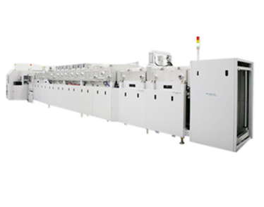
Shield sputter
(CNI)- Model:SIGMA1000、CURUS-C200、H-VAM
- Date:2016/5/12
- Email:sw@sellingware.com.tw
Nowadays, Electro-Magnetic Interference (EMI) Shield in the mobile device is raised as an critical issue according to the increase of semiconductor
package in the variable frequency. Conventionally, EMI shielding was performed at PCB substrate. But this traditional method has reached a
limitation at thinning and lightening. Therefore, paradigm about EMI shield is changing as the development of EMI shield method at semiconductor package level. Recently, CNI Technology has successfully developed inline sputtering system for deposition of EMI shield layers, and supplies
customized solution according to semiconductor package size.