Semiconductor Materials
-
Burn-in-Board
(ESA)- Model:The design for Aehr、Ando、 Jec 、 SSE system
- Date:2011/5/5
- Email:sw@sellingware.com.tw
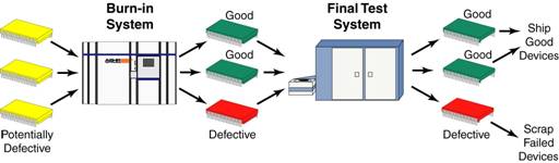
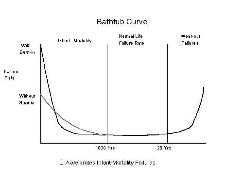
Burn-in is the process of stressing and exercising electrical devices to ensure optimum performance. This process forces defective semiconductor devices to fail before they are incorporated into assemblies where they can cause reliability problems in the end product.
Test & Reliability Screening Process
Burn-in can be done in different product development stages: engineering (design, reliability, or quality), and production. It can be performed on a small sample of devices, or all devices. You can burn-in unpackaged devices, packaged devices or devices mounted on PC boards. The most common method is to burn-in devices in production after packaging and before final test.