Back to List
PhysSemiconductor equipment
Si, SiC, GaN, GaAs bare wafer & epi wafer defect inspection
Model: NIR-PLuS
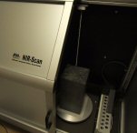
Product Information
Product NameSi, SiC, GaN, GaAs bare wafer & epi wafer defect inspection
BrandPhys
Product ModelNIR-PLuS
Sales Contactsw@sellingware.com.tw
Specifications
PL measurement is a non-contact, non-destructive measurement. Using PL can detect large-volume internal defects and impurities which cannot be detected by ordinary AOI equipment. Compared with general electrical measurement defects, PL has the advantages of fast speed, high resolution, and can be applied on both bare & Epi wafer inspection.
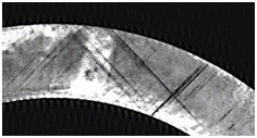
Si Slip Dislocation
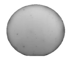
GaN缺陷檢測
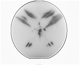
GaAs PL defect map
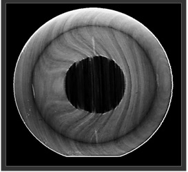
Si晶片生長缺陷

SiC map before KOH

Si growth impurity / Slips