Products

High-quality semiconductor materials and equipment for diverse applications

Found 34 products

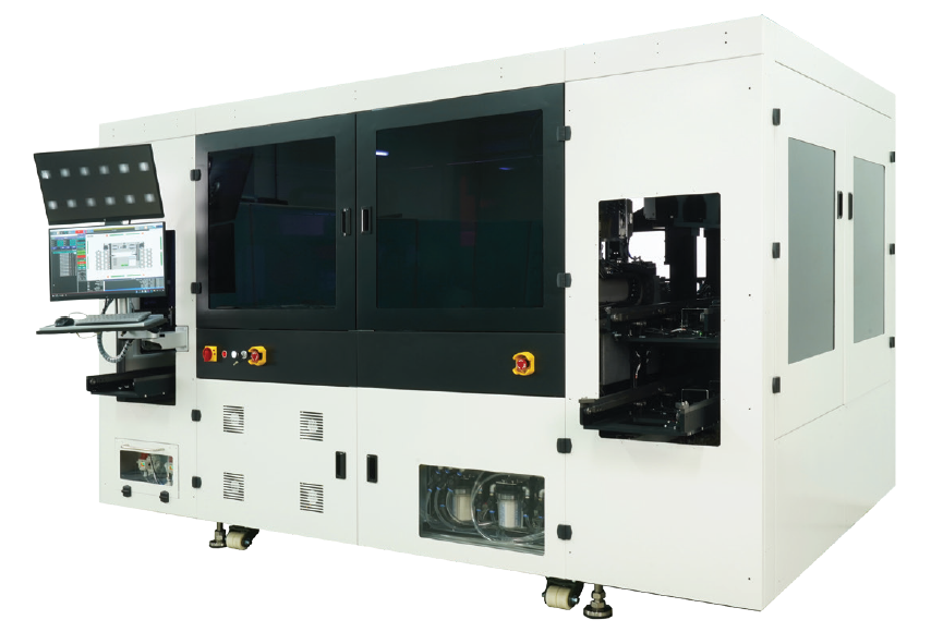
EddyCus® ResMapper
SURAGUS

EddyCus® ResMapper

Model: NA

The EddyCus® ResMapper is a fully automated chip imaging device (fully automated model) with an automated chip cassette handling system for full-area characterization of chip substrates or coatings to ensure process reliability and quality assurance in the semiconductor industry. The system is equipped with two non-contact eddy current sensors operating in transfer mode. This allows for highly detailed visualization of the uniformity of the substrate material or conductive coating. This device is typically used for: • Resistivity 0.1 – 100 mOhm-cm, • Board resistivity ranging from 0.0001 – 100,000 ohms/square, • Thin film metal layer thickness ranging from 2 nm to 1 mm, • Total thickness variation ranging from 300 – 1,000 µm and bow pitch ± 1 mm.

Burn-in-Board
ESA

Burn-in-Board

Model: The design for Aehr、Ando、 Jec 、 SSE system

Burn-in is the process of stressing and exercising electrical devices to ensure optimum performance. This process forces defective semiconductor devices to fail before they are incorporated into assemblies where they can cause reliability problems in the end product.

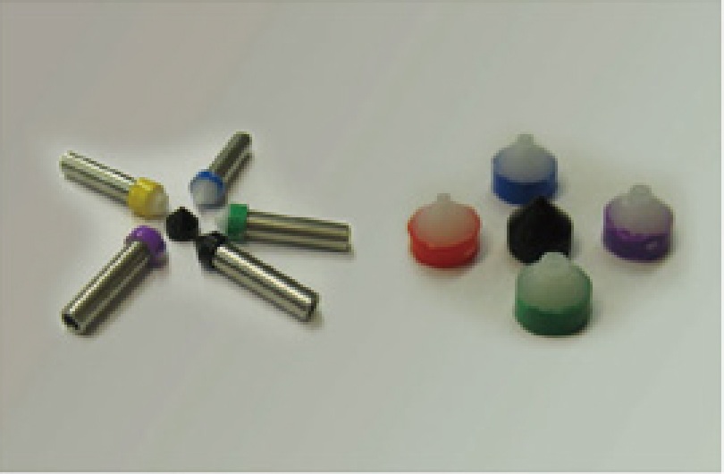
Rubber tip
R-SEMICON

Rubber tip

Model: RRN-XXX-XXX-1、RRN2-XXX-XXX-1、RRTHN-XXX-XXX-1、NHTR-XXX、RR-XXX-XXX-SB

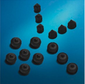
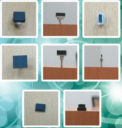
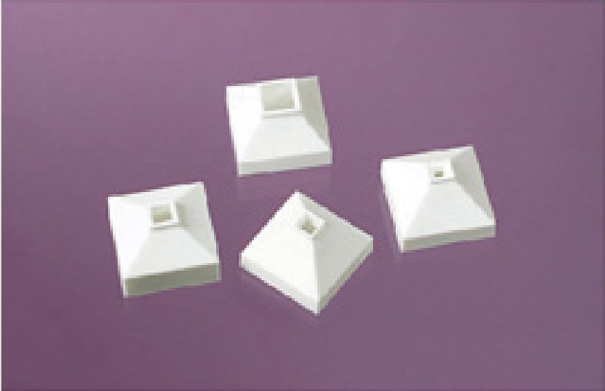
Description 1: Able to withstand up to 120℃. Suitable for epoxy Die-Attached and Pick N Place process. Description 2: Temperature withstand up to 300℃and intermittent exposures t0 450℃. Description 3: Square & Rectangular Rubber Tip for Picking-Up Along the Edges of Solder Bump Die (For Flip Chip process). CUSTOM MADE SIZE IS ALSO AVAILABLE. PLEASE CONTACT US FOR YOUR REQUIREMENT. Description 4: Multiple Holes Cross-groove Hi-Temp Rubber Tip For 2-3 Mils thin Die. CUSTOM MADE SIZE IS ALSO AVAILABLE. PLEASE CONTACT US FOR YOUR REQUIREMENT. Description 5: Able to withstand up to 120℃. Suitable for epoxy Die-Attached and Pick N Place process.

Multi Chamber Direct Plasma
Vision Semicon

Multi Chamber Direct Plasma

Model: VSP-88D Pro+

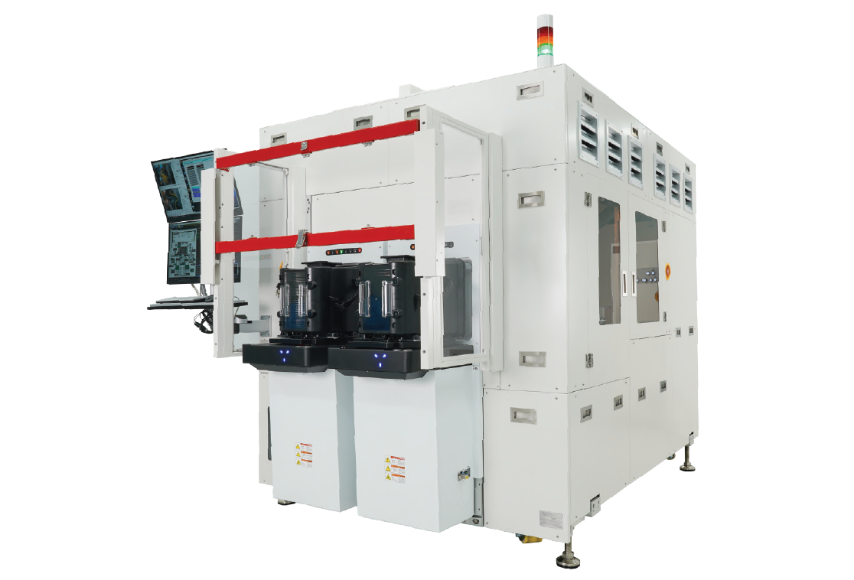
Products Description : Twin in-line system with magazine to magazine Easy magazine loading on conveyor Unique Chamber design (High clan ability & uniformity) High throughput capability with 4 lane transferring & short cycle time Simple utility connection design with Vertical UP/DOWN chamber movement Vacuum type plasma with small chamber Easy operation with touch screen operation & PC based main control Low price, low operation cost

Vacuum Shaping Device
矽菱醫材

Vacuum Shaping Device

Model: ME11W

Coverlay、3Layer CCL、Bonding Sheet、Stiffener
INNOX

Coverlay、3Layer CCL、Bonding Sheet、Stiffener

Model: MA series、MC&MD series、BS series、MS&SA series

Based on long experience in developing semiconductor materials, INNOX has developed FPC materials and successfully commercialized them as products like coverlay, FCCL, carrier film, bonding sheet and support board. INNOX has the complete INNOFLEX lineup that covers all sorts of FPC material. INNOX has constructed mass production systems standing on its own unique technologies in manufacturing FPC materials. INNOFLEX will meet your needs for both reliable products and satisfactory service.

Pressure Oven System
Vision Semicon

Pressure Oven System

Model: VSAO-1CM

Products Description : When bonding during process, it applies pressure and temperature to remove tiny void in adhesive and increases steady stiffness and adhesion by controlling void elimination Wafer Lamination,Die Bonding TC Bonding(Thermo compressing bonding) Dispensing / Printing / Potting,Via Filling Capillary underfilling / No flow underfilling,Reflow Features Temperature uniformity ± 3% Temperature control accuracy ± 0.1 ℃ Pressure: Max. 2.0MPa (20 kg/cm^2) 1st and 2nd pressure safety valves Digital Recording and Network application Temperature control and Multistep cure by control panel Parameter management by barcode LAN network and CIM PIM hard disk data storage IN/OUT Automatic indication on LCD monitor Excellent temperature control with superior temperature homogeneity Easy PC control program Easy to drive machine and manage data by its own software Sample protection by overheating prevention system Door open when power failure Acquired safety certificate of pressure vessel

Loc Tape、lead Lock Tape、Heat-Resistant PSA Tape、Spacer Tape、QFN Tape、WBL Film
INNOX

Loc Tape、lead Lock Tape、Heat-Resistant PSA Tape、Spacer Tape、QFN Tape、WBL Film

Model: ML&MZ series、MF series、PS series、HI-PST&HI-ST series、PQ series、WL series

INNOSEM is single or double-sided adhesive tape used in semiconductor assembly process for attaching leadframes to chips, or bonding metal circuits. Semiconductor tape requires high reliability in heat resistance, dimension stability and adhesiveness, on which the functions and reliability of semiconductor largely depend. This is why INNOSEM is produced under high-degree clean-room conditions comparable to those of semiconductor lines.Main ingredient is polymer, such as polyimide, epoxy, acryl, etc.

Needle
R-SEMICON

Needle

Model: EN-18-0.7-15-XXX、EN-18-0.7-30-XXX

Description 1: To push Die out from 100%SAWTHROUGH Wafer Tape. Suitable for Die size (Above 40X40 MILS). To reduce Microcrack Die problem. Description 2: To eliminate back Die Microcrack Problem.